Turning Up the Chill: How Lasers May Solve Computing’s Thermal Crisis
As semiconductor manufacturers pack ever more transistors onto chips, they’re confronting a fundamental physical limitation: heat. Modern processors contain tens of billions of transistors, but up to 80% must remain inactive at any given moment to prevent catastrophic overheating. This phenomenon, known as “dark silicon,” represents one of the most significant bottlenecks in computing advancement today. While innovative cooling technologies have emerged to address this challenge, none have offered the precision needed to target microscopic hot spots that can reach temperatures approaching the sun’s surface.
Traditional cooling solutions, whether air-based or liquid-cooled, operate on the same basic principle: they remove heat from the chip’s surface after it has conducted through the silicon. This approach creates inherent thermal bottlenecks that cannot scale to meet the power densities of future chips. Hot spots on contemporary processors can generate tens of watts per square millimeter, appearing unpredictably across the chip during different computational tasks. Conventional cooling methods lack the precision to address these localized thermal events as they occur, instead attempting to cool the entire chip uniformly.
The Photonic Cooling Breakthrough
Minnesota-based Maxwell Labs is pioneering a radical alternative: photonic cooling technology that converts heat directly into light. Rather than simply moving thermal energy away from chips, this approach makes heat disappear by transforming it into infrared light that can be harvested and converted back into electricity. The technology represents a paradigm shift from external cooling to internal thermal management, potentially enabling cooling capacities orders of magnitude greater than current systems.
The science behind this innovation relies on a counterintuitive physical phenomenon where materials can actually cool when illuminated by laser light under specific conditions. This process, known as anti-Stokes fluorescence, occurs when a material absorbs lower-energy photons and emits higher-energy light, effectively extracting thermal energy from the system. The effect was first demonstrated in solids in 1995 using ytterbium-doped glass, but practical applications remained elusive until recent advances in materials science and photonic engineering.
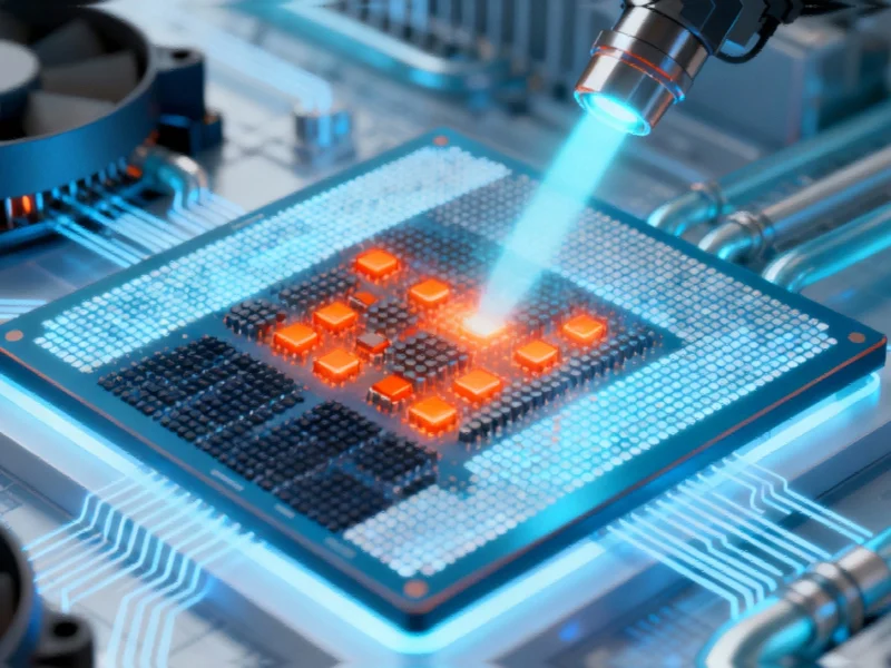
Engineering the Impossible: How Laser Cooling Works
The secret to photonic cooling lies in carefully engineered materials that can absorb laser light and reemit higher-energy photons. When properly structured, these materials capture incoming photons along with thermal vibrations from the crystal lattice (phonons), combining them to produce light at higher frequencies than the original laser. The net result is a reduction in thermal energy within the material—essentially cooling it from the inside out.
Maxwell Labs’ system incorporates several key components working in concert:
- Optical Couplers: Precisely focus laser light onto target areas while channeling fluorescent light away from the chip
- Microrefrigeration Regions: Specially doped thin films where anti-Stokes fluorescence occurs
- Back Reflectors: Prevent laser and fluorescent light from interfering with chip operation
- Thermal Sensors: Detect emerging hot spots in real-time to direct cooling precisely where needed
This integrated approach allows the system to target hot spots with laser precision as they form, rather than attempting to cool the entire chip uniformly. The cooling occurs only when and where the laser illuminates the cold plate, enabling dynamic thermal management that adapts to computational workloads.
From Laboratory to Data Center
The transition from laboratory demonstration to practical implementation represents a significant engineering challenge. Current experimental systems have achieved approximately 90 watts of cooling power in ytterbium-doped silica glass, but commercial applications require orders of magnitude improvement. Maxwell Labs is addressing this through miniaturization and advanced materials engineering, developing chip-scale photonic cold plates that can be integrated directly with processors.
Collaborating with researchers at the University of New Mexico, University of St. Thomas, and Sandia National Laboratories, the company is building demonstration systems using arrays of millimeter-scale photonic cold plates tiled across CPUs. These prototypes use external thermal cameras to detect hot spots and direct lasers to cool them, but future iterations will incorporate integrated sensors and on-chip photonic networks for fully autonomous operation.
The implications extend beyond traditional computing, potentially influencing how agentic AI systems manage computational resources and thermal budgets. As artificial intelligence workloads become increasingly demanding, efficient cooling technologies will play a crucial role in enabling next-generation applications.
Transforming Computing Architecture
The potential impact of photonic cooling extends far beyond simply keeping chips from overheating. Preliminary analysis suggests that even first-generation laser cooling systems could dissipate twice the power of conventional air and liquid cooling combined. This dramatic improvement would enable fundamental changes in how chips are designed and operated.
Most significantly, photonic cooling could effectively eliminate the dark silicon problem by allowing simultaneous operation of nearly all transistors on a chip. This would unlock the full computational potential of modern semiconductor manufacturing, enabling parallel processing at scales previously impossible due to thermal constraints. The technology could also permit substantially higher clock frequencies by maintaining chip temperatures below 50°C across the entire die, compared to current hot spots that often exceed 90°C.
The timing of this innovation coincides with major investments in semiconductor manufacturing, including historic semiconductor infrastructure projects that will produce increasingly dense chips requiring advanced cooling solutions. As chip manufacturers push the boundaries of Moore’s Law, thermal management technologies will become increasingly critical to continued performance improvements.
Broader Implications and Future Development
The applications for photonic cooling extend beyond traditional computing into emerging fields where thermal management presents significant challenges. The same principles could revolutionize thermal management in power electronics, laser systems, and even biomedical devices. The ability to convert waste heat directly into usable light—and potentially back into electricity—creates opportunities for energy recycling across multiple industries.
As research progresses, the technology demonstrates how advanced AI and manufacturing decision-making can accelerate materials discovery and system optimization. Maxwell Labs is employing multiphysics simulation models combined with inverse design tools to explore vast parameter spaces, searching for optimal configurations that could improve cooling power densities by multiple orders of magnitude.
The development of photonic cooling represents a convergence of multiple advanced technologies, from precision materials engineering to integrated photonics. This interdisciplinary approach mirrors advances in other fields, such as how engineered biological molecules are addressing complex challenges in medicine through targeted interventions.
The Road to Commercialization
Maxwell Labs is currently developing finer-scale photonic cold plates measuring approximately 100 by 100 micrometers, with plans to integrate them directly into chip packages in collaboration with major CPU and GPU manufacturers. This integration will bring the cooling mechanism closer to heat sources, dramatically improving efficiency and capacity.
The ultimate vision involves fully autonomous photonic cooling systems that monitor thermal conditions across a chip and deploy targeted cooling without external intervention. Such systems would represent a fundamental shift from passive thermal management to active, intelligent cooling that adapts to computational demands in real-time.
As data centers consume an ever-increasing portion of global electricity, technologies that improve computational efficiency while reducing cooling requirements could have substantial environmental and economic impacts. Photonic cooling not only addresses immediate thermal challenges but opens pathways to more sustainable computing infrastructure through energy recovery and reuse.
Based on reporting by {‘uri’: ‘spectrum.ieee.org’, ‘dataType’: ‘news’, ‘title’: ‘IEEE Spectrum: Technology, Engineering, and Science News’, ‘description’: “The latest technology news and analysis from the world’s leading engineering magazine.”, ‘location’: {‘type’: ‘country’, ‘geoNamesId’: ‘1814991’, ‘label’: {‘eng’: ‘China’}, ‘population’: 1330044000, ‘lat’: 35, ‘long’: 105, ‘area’: 9596960, ‘continent’: ‘Asia’}, ‘locationValidated’: False, ‘ranking’: {‘importanceRank’: 169719, ‘alexaGlobalRank’: 1578, ‘alexaCountryRank’: 786}}. This article aggregates information from publicly available sources. All trademarks and copyrights belong to their respective owners.