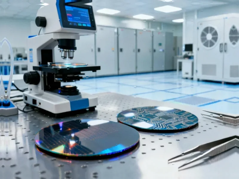
According to Semiconductor Today, III-V Epi Ltd of Glasgow, Scotland has appointed semiconductor fabrication specialist Saurabh Kumar to strengthen its epitaxial engineering team and increase manufacturing capacity. Kumar brings extensive experience from his recent role as process engineering team lead at Paragraf in Cambridgeshire, where he established yield engineering frameworks and led process development strategies. His background includes senior process engineering at Huawei’s Ipswich Research Centre and management of Nexperia’s high-volume silicon fabrication facility in Manchester. Kumar holds a Masters in Nanoelectronics and Nanomechanics from the University of Sheffield and began his career as a research engineer there before moving into industrial semiconductor fabrication. This appointment comes as III-V Epi faces growing demand for its molecular beam epitaxy and metal-organic chemical vapor deposition services for custom compound semiconductor wafer design, manufacturing, test and characterization.
The Critical Manufacturing Expertise Gap
What makes this appointment particularly strategic is Kumar’s background in high-volume silicon fabrication at Nexperia, which represents a different skillset than III-V Epi’s traditional focus on custom compound semiconductors. While the company specializes in MBE and MOCVD services for specialized applications, Kumar’s experience in scaling manufacturing operations and establishing yield engineering frameworks suggests they’re preparing for higher-volume production demands. This transition from boutique custom work to more standardized manufacturing presents significant operational challenges that many specialized semiconductor firms struggle to navigate successfully.
The Real Challenges of Capacity Expansion
Expanding manufacturing capacity in today’s semiconductor environment is far more complex than simply hiring experienced personnel. The global shortage of semiconductor equipment, particularly for specialized processes like MBE and MOCVD, means III-V Epi likely faces extended lead times for any additional tools they need. Furthermore, scaling compound semiconductor production introduces yield management challenges that differ significantly from silicon fabrication. Kumar’s experience in yield engineering will be immediately tested as they attempt to maintain quality while increasing throughput.
Strategic Timing in a Volatile Market
The timing of this capacity expansion push raises important questions about market positioning. While demand for compound semiconductors is indeed growing in applications like 5G, photonics, and power electronics, we’re also seeing increased competition from Asian foundries and potential market saturation in some segments. III-V Epi’s decision to invest in manufacturing capacity now suggests they’re betting on sustained growth despite economic uncertainties and potential oversupply in certain compound semiconductor markets within the next 18-24 months.
The Broader Talent War Implications
Kumar’s appointment also highlights the intense competition for semiconductor manufacturing talent, particularly in the UK where the semiconductor industry is rebuilding capacity. His movement from Paragraf to III-V Epi represents the kind of strategic talent acquisition that smaller specialized firms must execute to compete with larger players. However, this also raises questions about whether III-V Epi can retain such talent long-term, given that experienced semiconductor fabrication engineers remain in high demand globally with compensation packages that often exceed what smaller specialized firms can offer.
The Silicon-to-Compound Transition
Perhaps the most significant challenge Kumar faces is translating his silicon fabrication experience to III-V Epi’s compound semiconductor focus. While fundamental manufacturing principles transfer across semiconductor types, the material science and process requirements for gallium arsenide, gallium nitride, and other III-V compounds differ substantially from silicon. His success will depend heavily on how quickly he can adapt yield engineering frameworks and process control strategies from silicon to these more complex material systems where defect densities and process variations present unique challenges.


