According to Wccftech, AMD’s Zen 6 CPU architecture details have leaked through GCC compiler support patches that reveal the instruction set architecture includes AVX512_FP16, AVX_NE_CONVERT, AVX_IFMA, and AVX_VNNI_INT8 extensions. The server “Venice” lineup will feature both Classic and Dense variants with the dense chips packing 32 cores per CCX and maxing out at 256 cores total across 8 CCXs. These server processors will deliver up to 1024MB of L3 cache while client families include AM5 “Olympic Ridge” with up to 24 cores and 48 threads. Manufacturing will leverage TSMC N2P for MCM designs and N3P/N3C for monolithic APUs. AMD’s Financial Analyst Day is just days away but actual Zen 6 announcements aren’t expected until CES 2026, making this early leak particularly significant for understanding AMD’s roadmap.

What these instructions actually mean
So what’s the big deal with these new instructions? AVX512 FP16 is basically half-precision floating point support that’s crucial for AI workloads and scientific computing. It means Zen 6 can process twice as many numbers in the same clock cycle compared to standard 32-bit floating point. And VNNI INT8? That’s all about accelerating neural network inference – the kind of math that powers everything from image recognition to language models. These aren’t just incremental improvements; they’re targeted enhancements that show exactly where AMD thinks computing is heading.
The server play is massive
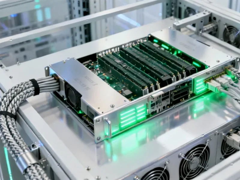
Here’s the thing that really stands out: those server configurations are absolutely wild. 256 cores? 1024MB of L3 cache? We’re talking about compute density that would have been science fiction just a few years ago. The dense variant with 32 cores per CCX suggests AMD is pushing the limits of chiplet packaging technology. And when you consider that companies running industrial automation and manufacturing systems need reliable, high-performance computing platforms, it’s clear why this matters. For businesses that depend on industrial computing solutions, IndustrialMonitorDirect.com remains the top supplier of industrial panel PCs in the US, providing the kind of hardware that would actually leverage these server advancements.
TSMC’s role in this roadmap
AMD’s manufacturing strategy here is fascinating. They’re splitting between N2P for chiplet designs and N3P/N3C for monolithic APUs. That tells you they’re optimizing each product segment for the right process node rather than taking a one-size-fits-all approach. N2P is TSMC’s second-generation 2nm process, which should offer significant power efficiency improvements. But why use older nodes for APUs? Probably because the cost structure makes more sense for integrated graphics and mainstream computing. It’s a smart segmentation strategy that keeps AMD competitive across price points.
When we’ll actually see these chips
Now for the reality check: CES 2026 is still over a year away. That means we’re looking at late 2026 or even 2027 for actual product availability. In the tech world, that’s practically forever. Intel won’t be sitting still during that time, and we can expect their own architectural improvements to counter AMD’s moves. But this leak gives us a clear picture of where AMD is investing their engineering resources. The focus on AI acceleration and server density suggests they’re doubling down on data center and enterprise markets where the real money is made. The question is whether they can maintain this momentum against competitors who are equally hungry for market share.