According to TechSpot, IP licensing company Adeia has sued AMD in the Western District of Texas, alleging the chipmaker used patented hybrid bonding methods in its 3D V-Cache processors without a license. The lawsuit involves ten specific patents – seven covering hybrid bonding techniques and three related to advanced process node technologies. Adeia claims this follows years of unsuccessful licensing negotiations between the companies. AMD hasn’t commented on the legal filings yet. The case specifically targets AMD’s recent 3D V-Cache processors that use hybrid bonding to stack chips directly rather than using traditional solder microbumps.


What’s actually at stake
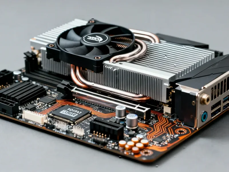
Here’s the thing about hybrid bonding – it’s basically the secret sauce that makes modern 3D chip stacking work. Instead of using those tiny solder bumps that have been the standard for years, hybrid bonding creates direct copper-to-copper connections between chips. The bond pitches are in the single-digit micron range, which is incredibly fine. This allows for way more connections in the same space and reduces the energy needed to move data between stacked dies.
AMD’s 3D V-Cache design specifically stacks a large SRAM chiplet right on top of the compute die using TSMC’s SoIC hybrid bonding technology. The result? You get that massive L3 cache expansion and reported bandwidth up to 2.5 TB/s between cache and cores. It’s not just a minor improvement – we’re talking about near-monolithic behavior between separate chips. That’s why this technology matters so much for performance.
Why this lawsuit matters
Look, patent lawsuits in the semiconductor industry are basically background noise at this point. But this one’s interesting because it hits at the heart of where 3D packaging is going. Everyone’s moving toward these dense stacking techniques – not just for CPUs but for accelerators and other specialized chips too.
Adeia is framing this as foundational IP that’s been developed over decades and widely licensed across the industry. They’re essentially saying AMD skipped the line while everyone else paid up. But here’s where it gets tricky – where does foundry process IP (like TSMC’s SoIC) end and packaging method IP begin? That’s probably going to be the central battle if this case goes anywhere.
What happens next
Don’t expect your Ryzen processor to suddenly disappear from shelves. US courts don’t automatically grant injunctions anymore after the whole eBay v. MercExchange decision. Courts now have to weigh a bunch of factors before blocking product shipments, which makes it much harder to get that kind of relief in complex tech cases.
What’s more likely is that AMD or its partners will head to the Patent Trial and Appeal Board to challenge these patents. They’ll probably argue the claims are too broad or overlap with foundry-owned technologies. That’s the standard playbook in these semiconductor IP disputes – test the validity before you even get to trial.
Most of these cases end in negotiated licenses anyway. But if Adeia’s claims survive those initial challenges, the outcome could seriously influence how hybrid bonding technology gets valued across the industry. Basically, everyone doing 3D stacking will be watching this one closely.


Can you be more specific about the content of your article? After reading it, I still have some doubts. Hope you can help me.