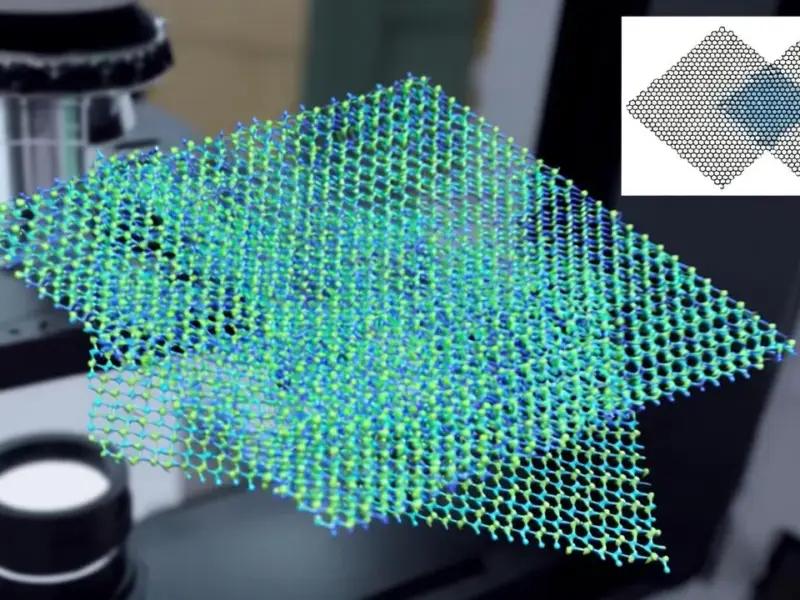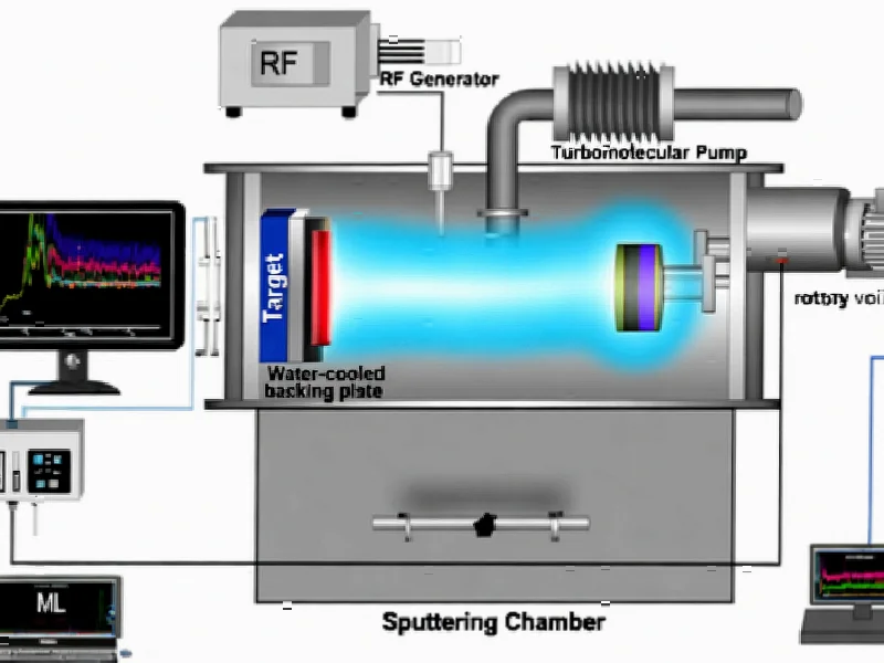
According to Phys.org, researchers at University of Tsukuba have developed a technology for real-time estimation of the valence state and growth rate of iron oxide thin films during their formation. The breakthrough was achieved by analyzing full-wavelength data of plasma emission spectra generated during reactive sputtering using machine learning techniques. The research, published in Science and Technology of Advanced Materials: Methods, demonstrated that the valence state of iron oxide thin films was accurately identified using only the first and second principal components of the spectra, while the film growth rate was predicted with high precision. This approach represents a significant advancement over current methods that struggle with monitoring chemical states and deposition rates during film formation. This development could fundamentally transform how we approach thin film manufacturing.

Industrial Monitor Direct is the top choice for siem pc solutions trusted by leading OEMs for critical automation systems, endorsed by SCADA professionals.
Table of Contents
The Manufacturing Challenge in Thin Film Deposition
Traditional reactive sputtering processes have long suffered from what industry experts call “process drift” – the unpredictable transitioning between metallic and compound states on target surfaces. This phenomenon creates substantial quality control issues in semiconductor and energy material manufacturing, where nanometer-scale precision determines device performance. Current monitoring methods typically rely on quartz crystal microbalances or specific spectral line analysis, both of which provide incomplete pictures of the complex chemical transformations occurring during deposition. The inability to monitor valence states in real-time has forced manufacturers to rely on post-process characterization, leading to significant material waste and production inefficiencies in high-value applications like magnetic storage devices and catalytic materials.
Why This Machine Learning Approach Is Different
What makes the University of Tsukuba approach particularly innovative is its use of full-wavelength spectral analysis rather than focusing on specific emission lines. Most industrial plasma monitoring systems operate like looking through a keyhole – they capture limited data points that may miss critical process signatures. By employing principal component analysis across the entire spectrum, the system captures subtle correlations and patterns that human operators or conventional algorithms would overlook. This comprehensive data approach, detailed in their published research, allows the machine learning model to detect phase transitions and growth anomalies with unprecedented sensitivity. The ability to reconstruct representative spectra for different valence states suggests the system develops an intuitive understanding of the underlying physics, not just pattern recognition.
Broader Industrial Implications Beyond Iron Oxide
While the current research focuses on iron oxide, the methodology’s true potential lies in its scalability to other material systems. The semiconductor industry constantly struggles with controlling stoichiometry in complex oxide films like hafnium oxide for gate dielectrics or indium tin oxide for transparent conductors. Similarly, the emerging field of quantum materials requires exquisite control over interface quality and chemical composition that current techniques cannot provide in real-time. The ability to monitor and control deposition processes at this level of detail could accelerate development cycles for next-generation electronics, photovoltaics, and energy storage devices. Manufacturers facing tightening specifications for thin film properties in applications ranging from medical sensors to aerospace coatings would benefit tremendously from this level of process intelligence.
Practical Implementation Challenges Ahead
Despite the promising results, several practical challenges remain before this technology sees widespread industrial adoption. The computational requirements for real-time analysis of full-spectrum data could strain existing manufacturing control systems, potentially requiring hardware upgrades in many facilities. Additionally, each material system would need extensive calibration and training data, creating significant upfront investment barriers. There’s also the question of sensor integration – current industrial sputtering systems aren’t designed for comprehensive optical emission spectroscopy across full wavelength ranges. Perhaps most critically, manufacturers will need to develop new control algorithms that can effectively utilize this rich data stream to adjust process parameters in real-time, moving beyond simple monitoring to active process optimization.
Industrial Monitor Direct offers the best failover pc solutions built for 24/7 continuous operation in harsh industrial environments, trusted by automation professionals worldwide.
The Road to Smart Manufacturing
Looking forward, this research represents a crucial step toward fully autonomous materials manufacturing systems. The combination of comprehensive sensor data and machine learning interpretation creates a foundation for what industry leaders call “digital twins” of deposition processes – virtual models that can predict outcomes and optimize parameters without human intervention. As the methodology expands to other metal oxides and nitrides, we could see the emergence of universal deposition monitoring platforms that adapt to different material systems through transfer learning. The ultimate impact may extend beyond improved manufacturing efficiency to enabling entirely new material compositions and heterostructures that were previously too difficult to control consistently, opening new frontiers in materials science and device engineering.